Realizing semiconductor contact probes thinner than a human hair with micromachining technology using CNC lathes
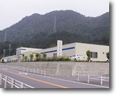
AIKOSHA CO., LTD.
"Even smaller and even lighter every day-our quest for ultrafinemachining technologies has no end."
Realizing semiconductor contact probes thinner than a human hair with micromachining technology using CNC lathes
AIKOSHA CO., LTD.
"Even smaller and even lighter every day-our quest for ultrafinemachining technologies has no end."
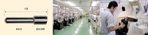
The World's smallest semiconductor contact probes (0.03 mm) realized by ultrafine machining technologies
During the manufacturing process, semiconductors are put through function tests. A tester is placed in contact with the electrodes of the semiconductor and the electric signals are measured. The pin-shaped element of the tester that is put in contact with the semiconductor is called the "contact probe."
As semiconductor circuits have become more and more highly integrated, the diameter of the contact probe has become smaller and smaller. Today, the majority of these contact probes are 0.4 mm in diameter. Aikosha, having launched probes of 0.03 mm, one of the thinnest in the world, is one of the key players supporting the semiconductor industry.
Contact probes have to be very thin, but their points have to be shaped into various forms such as a cone, a pyramid, or a crown, according to the type of probe. Aikosha is known for its unique technologies for various processing, such as shaving extremely thin probes even thinner, machining the point, and then drilling this point according to the form of the semiconductor with a CNC lathe having special blades.
Starting as a clock manufacturer, Aikosha has successfully changed its business direction into the production of semiconductors and similar products, building on the precision machining technologies it had acquired. Young technicians operate state-of-the-art machines to take over the manufacturing skills of senior craftsmen.
Taking on challenges for the ultrafine machining technologies of the 21st century
In the near future, with Southeast Asian countries expected to nip at our heels in the manufacture of contact probes for semiconductors, Aikosha tries to stay ahead of its competitors by launching technologically superior products like ultrafine probes and high-current compatible probes. It has already succeeded in prototyping probes of 0.02 mm and is trying to make ones even thinner expecting that, in a decade from now, there will be a demand for probes of 0.01 mm.
At the same time, the company is working to bring their ultrafine cutting technologies to an even higher stage to respond to demands from new fields, such as for information devices, medical equipment, and auto parts.
Company Profile
(All information and data are as of May 2005.)